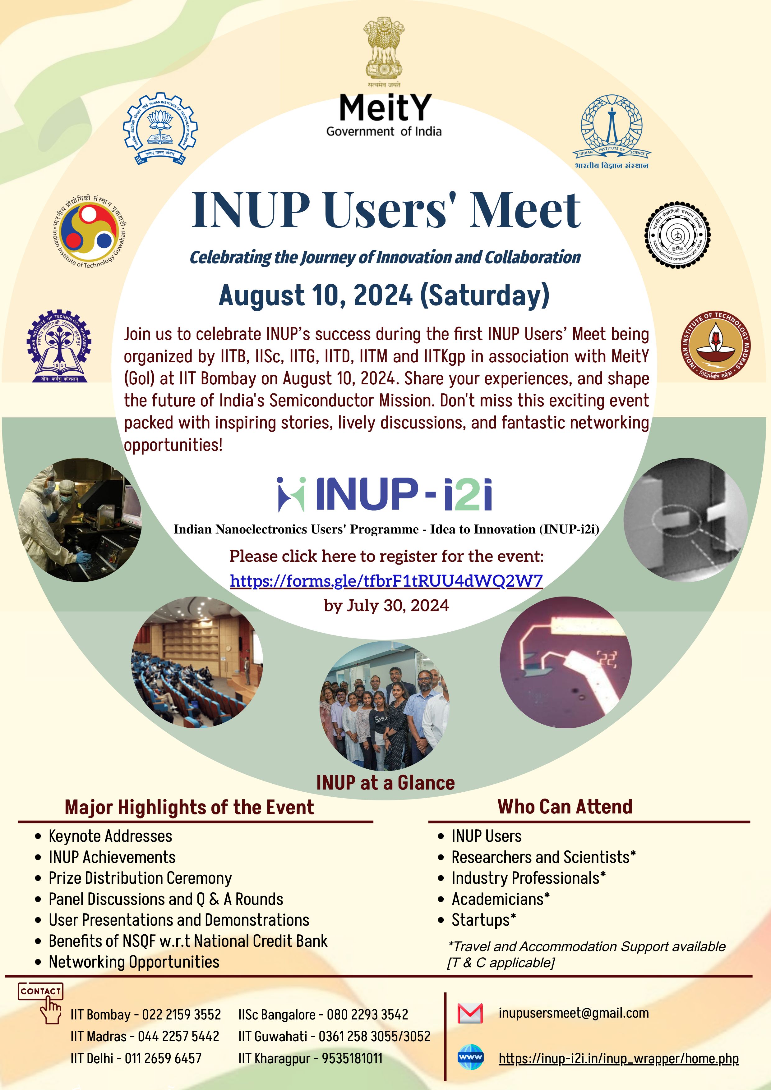
Celebrating the Journey of Innovation and Collaboration
On 10th August, 2024 (Saturday)
Please click here to give your valuable feedback on INUP program.
Speaker : Generation of Semiconductor Talent
Date & Venue : 28-03-2025 & IIT Bombay
About the workshop : Sunit Rikhi, a SemiX Executive, delivered an insightful talk on "Careers in Semiconductor Manufacturing" at COEP Technology University. 200+ bright and curious students engaged in a dynamic discussion and interactive Q&A, exploring the exciting career opportunities in India's growing semiconductor industry. With such enthusiasm from future engineers, India Semiconductor Mission is in great hands! Let's keep the momentum going collaborating with academia and industry to build a strong, skilled workforce for India's semiconductor revolution.
Speaker : Industry-University Partnership Talk at SemiX, IIT Bombay
Date & Venue : 25-03-2025 & IIT Bombay
About the workshop : On February 24, 2025, we hosted an insightful talk by Dr. Sameer Pendharkar, Vice President and Senior Fellow, Technology Development at Texas Instruments Inc., on "Industry-University Partnership – Bringing New Technology to Market."
Speaker : Prof. T. Venkatesan's Colloquium at SemIX, IIT Bombay
Date & Venue : 17-03-2025 & IIT Bombay
About the workshop : SemiX had the privilege of hosting Prof. T. Venkatesan, a trailblazer in Pulsed Laser Deposition (PLD) and semiconductor innovation, from the University of Oklahoma. The colloquium was inspiring, sparking ideas that could redefine the future of semiconductor research and education in India.
Speaker : Evolution of System Architecture: Decision-Making
Date & Venue : 11-02-2025 & IIT Bombay
About the workshop : In-depth insights into Intel CPU-based architectures: Nitin expertly guided us through the architectural principles and crucial trade-offs that shape modern computing.
Speaker : Semiconductor Storage Technologies
Date & Venue : 24-01-2025 & EE301, GG Building, IIT Bombay
About the workshop : On January 24, 2025, we had the pleasure of hosting an engaging talk on Heat-Assisted Magnetic Recording (HAMR) by Dr. Stephanie Hernandez at IIT Bombay. The session was attended by enthusiastic students and faculty members deeply involved in magnetic memories.
Speaker : Role of Advanced Film Deposition Technology
Date & Venue : 07-01-2025 & GG301, Seminar Room, 3rd Floor, GG Building, EE Department, IIT Bombay
About the workshop : The talk on the "Role of Advanced Film Deposition Technology to Enable Future of Patterning" presented by Sudipto Naskar from Intel Corporation, was successfully held on January 7, 2025. The session was well-attended by students, faculty members, and technical staff. All participants were eager to delve into the advances of semiconductor technology. During the talk, Sudipto Naskar shared valuable insights into current research and the challenges faced in advanced film deposition. He emphasized the critical need for industry-academia collaboration and innovation. He invited researchers to engage in finding solutions to pressing technological issues in Film Deposition Technology. This talk was made possible by the proactive initiatives of Prof. Saurabh Lodha and Vijay Mishra. We are committed to bringing more enlightening learning opportunities. Thank you to everyone who participated and contributed to a vibrant discussion! We look forward to seeing more collaborative efforts to address the future challenges of semiconductor technology.
Speaker : Biology Needs Computer Architects
Date & Venue : 24-11-2024 & EEG301, Seminar Room, 3rd Floor, GG Building, EE Department, IIT Bombay
About the workshop : Today we had the privilege of hosting Sneha Goenka, an esteemed IIT Bombay alumna IIT Bombay Alumni Association (IITBAA), for an insightful talk on advanced computational tools in genomics. Key Highlights: A Step Towards Industry-Academia Collaboration This talk was part of our ongoing efforts to foster student-industry interactions at Elctrical Engineering Dept. of Indian Institute of Technology, Bombay. The recent demonstration of these tools marks a significant milestone in enhancing collaboration in semiconductor technology. Conducted under the Electrical Engineering program by Prof. Udayan Ganguly and Prof. Siddharth Tallur, this event attracted a diverse audience of advanced undergraduate, postgraduate, PhD students and SemiX staff members.
Speaker : EduTwin Platform
Date & Venue : 24-10-2024 & EEG 301
About the workshop : In this session, we discussed the vision of EduTwin™ as a virtual classroom dedicated to semiconductor hardware, processes, and integration learning. We introduced two key components of the platform: ACE+: Focused on multiphysics and multiscale modelling. TOPO+: Designed for topographical modelling of features. Get ready to explore fascinating case studies showcasing how these innovative tools tackle pressing process challenges in semiconductor device performance and yield.
Speaker : Neuromorphic Computing Overview and Results
Date & Venue : 20-09-2024 & GG301, Seminar Room, 3rd Floor, GG Building, EE Department, IIT Bombay
About the workshop : The term "neuromorphic computing" is interpreted in various ways by different people. In this talk, I will present our view on the matter from the perspective of the Intel Loihi architecture. I will also present an overview of the results obtained using Loihi and Loihi 2 chips. If time permits, we will take a brief look at the architecture of the chips as well as some details about how to engage with the Neuromorphic Community built around Loihi.
Speaker : freedom of 2D exciton
Date & Venue : 22-05-2024 & Seminar Room GG301, GG Building, 3rd Floor, Department of Electrical Engineering, IIT Bombay
About the workshop : Monolayer semiconductors and their van der Waals heterojunctions are excellent testbeds to study chirality dependent light-matter interaction at the nanoscale. In this talk, I shall discuss our recent results on pushing the exciton emission linewidth and its valley coherence in monolayer semiconductors to the fundamental limits. In particular, I shall show experimental techniques to achieve ~100% valley coherent exciton, and emission linewidth close to the homogeneous broadening limit. I shall also show evidence of “motional narrowing” effect in exciton polarization, which leads to a counterintuitive improvement of valley coherence and valley polarization at higher exciton scattering rates. Time permitting, towards the end of the talk, I shall give an overview of our recent efforts on developing quantum hardware components, such as, single photon emitter, single photon detector, and quantum random number generator.
Speaker : Here come Semiconductor Fabs! What are these? And what must our response be?
Date & Venue : 17-04-2024 & Lecture Hall 21, Second Floor, Victor Menezes
About the workshop : Despite its 60-year history, the semiconductor industry has recently experienced a surge in global interest due to supply chain disruptions during the Covid years. This has led to a race among nations to secure strategic positions in this growing industry, and India is actively participating. Recent announcements have set India Fab plans in motion. This talk is prepared for audiences at IIT Bombay who want to understand the structure, operations, success measures, and challenges of semiconductor manufacturing and its ecosystem. Although we will explore the inner workings of semiconductor manufacturing, we will stay at a high level and use a broad brush to benefit students, faculty, and administrators from any engineering discipline at IIT Bombay. We will also discuss how the fledgling Center of Semiconductor Technologies (SemiX) at IIT Bombay can help secure India’s desire to be a global semiconductor manufacturing hub.
Speaker : Analog Circuits Based on Digital-Assisted Techniques
Date & Venue : 10-04-2024 & EEG 301 GG Building, Department of Electrical
About the workshop : In this talk, we will present digitally assisted analog techniques to enhance the performance of high-precision analog circuits like ADCs, DAC, and low noise bandgap reference. Due to the advantages of sampling noise, continuous time-pipelined ADC is an emerging architecture. However, the images and realizing delay in continuous time and stringent matching constraints limit those performances. We will present you a hybrid continuous pipelined and delta-sigma architecture where we harness the anti-alias feature of DSM to suppress the images. Further, one-time calibration techniques are presented to both the flash ADC and DAC, which has a tempco of almost zero. Schematic simulation shows an enob of 16 bits in 20MHz bandwidth while consuming 31mA from a 1.8V supply. A current steering DAC implemented in 65nm achieves an SFDR > 80dB while outputting a 40mA signal current at 3GHz. Continuous current cell calibration results in a matching of about 16 bits. High-speed B2T architecture with inherent DEM capabilities converts the timing mismatches to the noise floor. Finally, we will present a digitally assisted bandgap architecture that does not use chopping and achieves a measured noise of 600 nV/sqrt (Hz) at 1Hz offset.
Speaker : Technological & Reliability Challenges of pGaN Gate
Date & Venue : 15-02-2024 & Seminar Room EEG 301, 3rd floor, GG Building, Electrical Engineering Department
About the workshop : Part 1:The first part of the talk will address the design, technology, and reliability challenges in pGaN gate-based e-mode HEMT technology and the technological achievements made by my group in IISc. In the second part of this talk, I will talk about a significant positive shift in the threshold voltage by integrating high-k AlxTi1-xO based p-type oxide in AlGaN/GaN HEMT gate stack and how it enabled 600V e-mode GaN HEMTs with superior gate control over channel and ON-state performance. In the third part of the talk, I will discuss the physics of dynamic On-resistance in AlGaN/GaN HEMTs and how the same can be suppressed using p-type AlTiO-based passivation. In the end, I will briefly touch base on some of the other key reliability physics contributions.
Speaker : Engineering Ultrawide
Date & Venue : 12-02-2024 & GG Conference room, 2nd Floor, GG Building, EE department
About the workshop : At the heart of rapidly evolving electronic devices is a meticulously engineered semiconductor material system. Atomic-level defects play a fundamental role in controlling the properties of semiconductors. Often, the level at which these defects need to be engineered can be as small as parts per billion. My research grapples with this formidable challenge by drawing on tools and concepts from thermodynamics and kinetics to develop predictive frameworks for systematic defect management, thereby enabling pathways for cutting-edge technologies. With the ubiquitous demand for higher-power electronics, shorter wavelength optoelectronics, and faster computing than what the incumbent technologies offer my research aims to implement ultrawide (>4.5 eV) bandgap (UWBG) semiconductors for developing next-generation electronic devices. The success of these new-generation semiconductor technologies hinges on the ability to overcome several, unique material and device challenges that become more pronounced as the bandgap increases. In this seminar, I will discuss how my research addresses this conundrum by encompassing several domains ranging from epitaxial growth, design, fabrication, and characterization of these devices with an emphasis on point defect management, structure-property correlations, and carrier transport physics. I will share several examples where such an approach to integrate materials science, physics, and electrical engineering allowed us to demonstrate cutting-edge devices while also striving toward boosting the performance to the theoretical limit, thus unlocking the consummate potential of UWBG semiconductors to enable disruptive technological changes.
Speaker : Applications and Heterogeneous Integration
Date & Venue : 12-02-2024 & LH 302 classroom, Lecture Hall Building IITB
About the workshop : This talk will attempt to establish a roadmap for 2-Dimensional (2D) material-based Nanoelectronic technologies for beyond Si and other future/disruptive applications with a vision for the semiconductor industry to enable a universal technology platform for heterogeneous integration. The heterogeneous integration would involve integrating orthogonal capabilities such as different forms of computing (classical, neuromorphic and quantum), all forms of sensing, digital and analog memories, energy harvesting, etc. – all in a single chip using a universal technology platform. This talk will also cover the technological and fundamental challenges in pushing the 2D technology to the market, where the world stands today, and what gaps are required to be filled. Talking about the gaps, I will particularly touch base on the Metal (3D) to graphene/TMD (2D) contact engineering challenges, which has been considered as one of the most fundamental challenges towards harnessing the full potential of 2-dimensional materials. And, how the fundamental understanding of the contact’s quantum chemistry resulted in unique ways to engineer it, resulting into record transistor performance. Besides, I will talk about some of the fundamental process challenges which can unintentionally perturb the 2D channel’s electrical, optical and mechanical properties. In the end, I will talk about some of the reliability gaps, which are urgently required to be addressed and the fundamental understanding we have developed so far.
Speaker : SemiX hosted a talk IIT Bombay
Date & Venue : 09-02-2024 & IIT Bombay
About the workshop : SemiX hosted a talk by Prof. Bhaswar Chakrabarti, Electrical Engineering Department, IIT Madras on Feb 9th. He talked on \"Volatile resistance switching in memristive devices for dendritic computation\"
Speaker : SemiX hosted Sunil Shenoy IITB
Date & Venue : 22-01-2024 & IIT Bombay
About the workshop : SemiX hosted IITB distinguished Alum Sunil Shenoy on 12th January for a talk. In his talk, he described his professional journey – A Walk Down
Speaker : Micron Technology team visit SemiX IIT Bombay
Date & Venue : 19-01-2024 &
About the workshop : We got an opportunity to interact with the leadership of the Micron Technology team on January 19. They visited our research facilities and discussed their future roadmap for engaging with SemiX IIT Bombay. Micron Technology Udayan Ganguly, Anand Ramamoorthy Chittoor Ranganathan Parthasarathy Swaroop Ganguly Nagasubramaniyan Chandrasekaran
Speaker : UC Santa Barbara
Date & Venue : 11-12-2023 & Lecture Hall 21, 2nd floor, VMCC, IIT Bombay
About the workshop : This talk will give an overview of the unique College of Engineering renowned for its collaborative culture and its ability to translate science, through innovation to technology in the service of society. It does so because of the hyper-connected faculty and shared facilities and welcoming environment for academics and industry. The College exemplifies the value of teamwork over siloed excellence, and I will share my own journey to illustrate how it has helped me and my students achieve their professional dreams. I hope the talk inspires creative, passionate and inspired students to choose UC Santa Barbara for their Ph.D. education and as a launchpad for an exceptional professional career.
Speaker : Semiconductor Lab for Virtual Fab Solutions
Date & Venue : 26-11-2023 & IIT Bombay
About the workshop : The Synopsys Semiconductor Lab for Virtual Fab Solutions, a flagship initiative of Synopsys Academic & Research Alliances at IIT Bombay, was inaugurated on November 26th by Shri Bhuvnesh Kumar, Additional Secretary, MeitY.
Speaker : Chiplets for AI/ML Applications
Date & Venue : 09-11-2023 & GG Conference Room, GG Building, Department of Electrical Engineering
About the workshop : This presentation delves into the significance of chiplets in hyperscaler data centers, focusing on their role in the dynamic field of AI/ML. The content traces the evolution of neural networks, emphasizing their importance in hyperscale computing environments, exemplified by companies like Meta Inc. Key applications of neural networks in hyperscalers, such as data mining on social media, multilingual translation, and a diverse range of AI/ML workloads encompassing ranking algorithms, computer vision, and natural language processing, are explored. An understanding of this diverse workload spectrum is essential for grasping the specific challenges and advantages of chiplet technology. In the era of AI, the computational landscape has undergone a transformation, characterized by the distinction between sparse and dense computations. This presentation sheds light on the immense computational demands of training large language models (LLMs), which necessitate yottabytes of data and domain-specific accelerators. The central focus of this discussion revolves around the chiplet advantage. It examines how chiplets enable efficient memory connections and facilitate architectural modifications, making them pivotal in optimizing the performance and efficiency of AI/ML workloads within hyperscaler data centers. This talk offers valuable insights into the “why, what, and how” of chiplets for AI/ML applications in hyperscaler data centers.
Speaker : Computing with Cadence Tensilica Processors: An Overview
Date & Venue : 03-10-2023 & GG Conference Room, GG Building, Department of Electrical Engineering
About the workshop : Differentiated hardware tailored to the application requirements is absolutely essential to achieve optimal performance and energy efficiency. Creating domain-specific processors for given application needs is key to navigate challenging area-power-performance metrics in SoC designs. In this talk, we introduce Cadence Tensilica’s Xtensa processor and TIE (Tensilica Instruction Extensions) technology for developing Application Specific Instruction Processors and related software tools. This patented technology is around for more than two decades and is silicon proven across semiconductor nodes from 90nm to cutting edge 5nm, with more than billion chips shipped every year. TIE language can be used to design variety of processors like VLIW, SIMD, Vector floating point which are tailored for application domains like Audio, Radar, Wireless Communications, Computer Vision and AI.


